Marten Electric 電気テン @ Home
Vintage audio gear connoisseur, computer enthusiast, time nut, music lover, vintage games gamer, nerd, tinkerer and shady electronic projects makerZilog Z80 CPU NOP Tester
Introduction
I have originally designed this PCB for my Z80 microcomputer project (WIP), but this turn out so well that I have now posted all schematic, gerber files and documentation to fellow enthusiast such as yourself :) Perhaps (and I hope) content in this obscured corner of interwebs will inspire you to start your own projects.
My CPU Tester project was inspired on 8Bit-Museum Stephan Slabihoud's Z80 NOP Tester I definitely recommend going through his webpage!
This is a simple Z80 CPU tester which exclusively executes NOP (No Operation) instructions to just check for basic functionality tests that the CPU can execute instructions. In addition it gives an indication if the clock input responds correctly.
Tester will not test all address lines and every function on the Z80, but gives you a quick indication if your treasure is good, bad or ugly. This little widget can also be used as easy to understand learging tool as it's minimal computer in itself. You might learn basics about how CPU works by observing system control lines linked to LED’s.
The CPU tester works with all NMOS and CMOS types of Z80 CPUs and compatible clones.
Design overview
What is NOP instruction?
NOP does nothing for 4 clock cycles. It is Useful for a short time waster (for example, it's common to put 8 clock cycles between output and input from the Key Port).
A NOP is most commonly used for timing purposes, to force memory alignment (may be used for pipeline synchronization), to prevent hazards, to occupy a branch delay slot, to render void an existing instruction such as a jump, as a target of an execute instruction, or as a place-holder to be replaced by active instructions later on in program development (or to replace removed instructions when reorganizing would be problematic or time-consuming).
Instruction mnemonic: NOP, Bytes: 1, Opcode 0x00, Notes: There are some other instructions without any effect (and the same timing): LD A, A, LD B, B etc.
How does it all work?
All data bus pins (A0-A7) are pulled to ground by pull-down resistors and the CPU executes NOP instructions (opcode 0x00) when the memory is read in an endless loop. The CPU starts executing these commands from address 0 after reset or data jump.
Addresses A0 to A7 are connected to LED's for visual display and will pulse on and off when the memory locations are checked. If the CPU executes the NOPs, the addresses A0 to A7 should be continuously incremented and CPU acts as a crude BCD counter, where A0 = 1, A1 = 2, A3 = 4, A4 = 8 and so on. You might be spooked by LED A7 flashing. Please don’t be, this is a standard artifact. Z80 executes a periodical memory refresh cycle, where memory access and memory refresh run synchronously.
The clock signal is generated by a 555 timer with variable frequency from 1 - 1200 Hz, so you can determine if the Z80 is executing instructions at different clock speeds. Address locations A0 - A7 are tested in about 3 seconds (1 operation per 4 cycles).
Please be aware, that since the CPU is under-clocked below specification, it is quite possible that in extreme cases the NOP tester might give you incorrect indication.
But what are all the LED’s for anyways?
M1 - Machine Cycle One (output, active Low). M1, together with MREQ, indicates that the current machine cycle is the op code fetch cycle of an instruction execution. M1, when operating together with IORQ, indicates an interrupt acknowledge cycle.
MREQ - Memory Request (output, active Low, tristate). MREQ indicates that the address bus holds a valid address for a memory read or a memory write operation.
IORQ - Input/Output Request (output, active Low, tristate). IORQ indicates that the lower half of the address bus holds a valid I/O address for an I/O read or write operation. IORQ is also generated concurrently with M1 during an interrupt acknowledge cycle to indicate that an interrupt response vector can be placed on the data bus.
RD - Read (output, active Low, tristate). RD indicates that the CPU wants to read data from memory or an I/O device. The addressed I/O device or memory should use this signal to gate data onto the CPU data bus.
WR - Write (output, active Low, tristate). WR indicates that the CPU data bus contains valid data to be stored at the addressed memory or I/O location.
CLK - Clock (input). Single-phase MOS-level clock. Four clock cycles per one machine cycle operation.
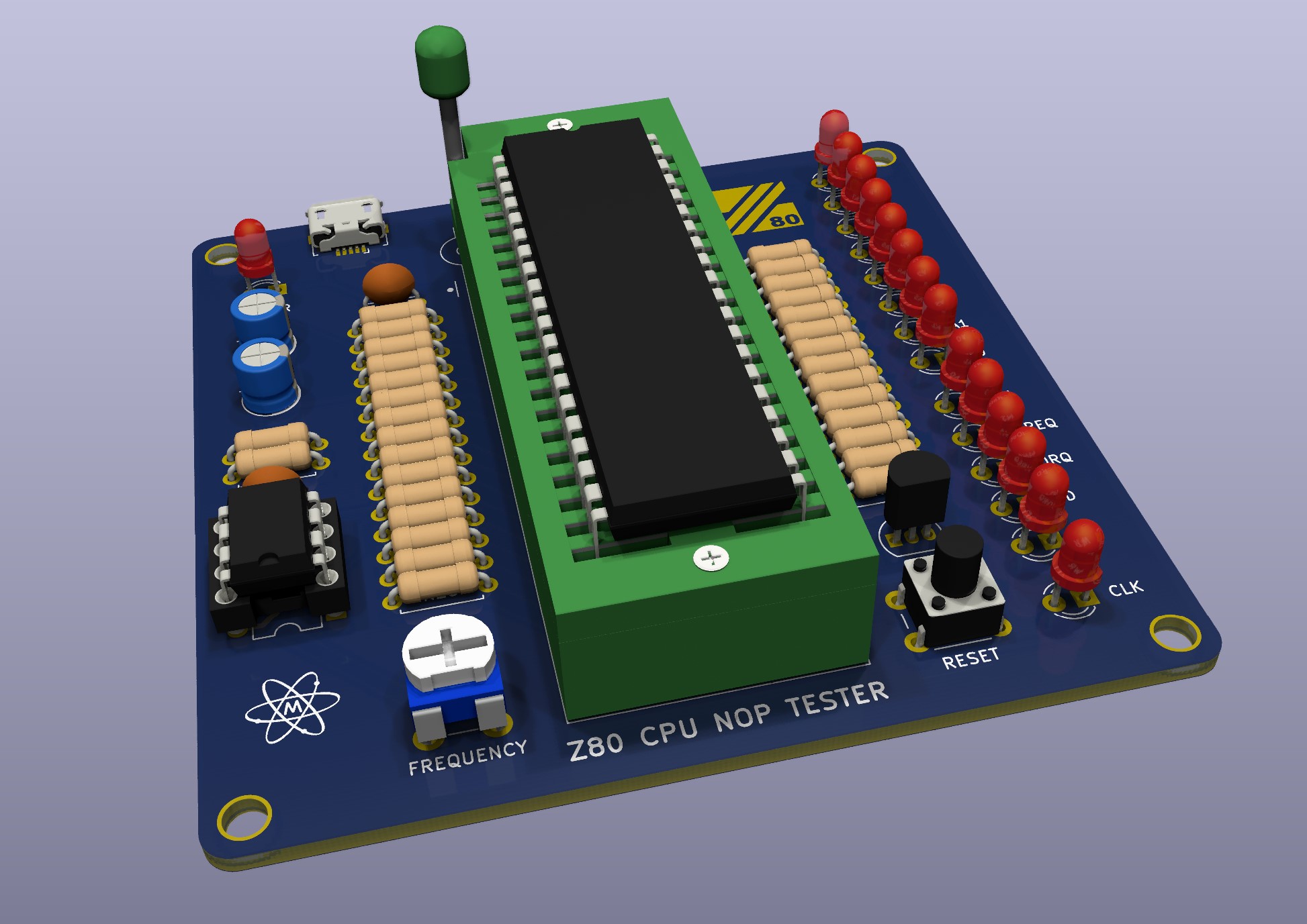
You can use CPU tester in conjuction with Z80 QFP44 to DIP40 and/or PLCC44 to DIP40 adaptors.
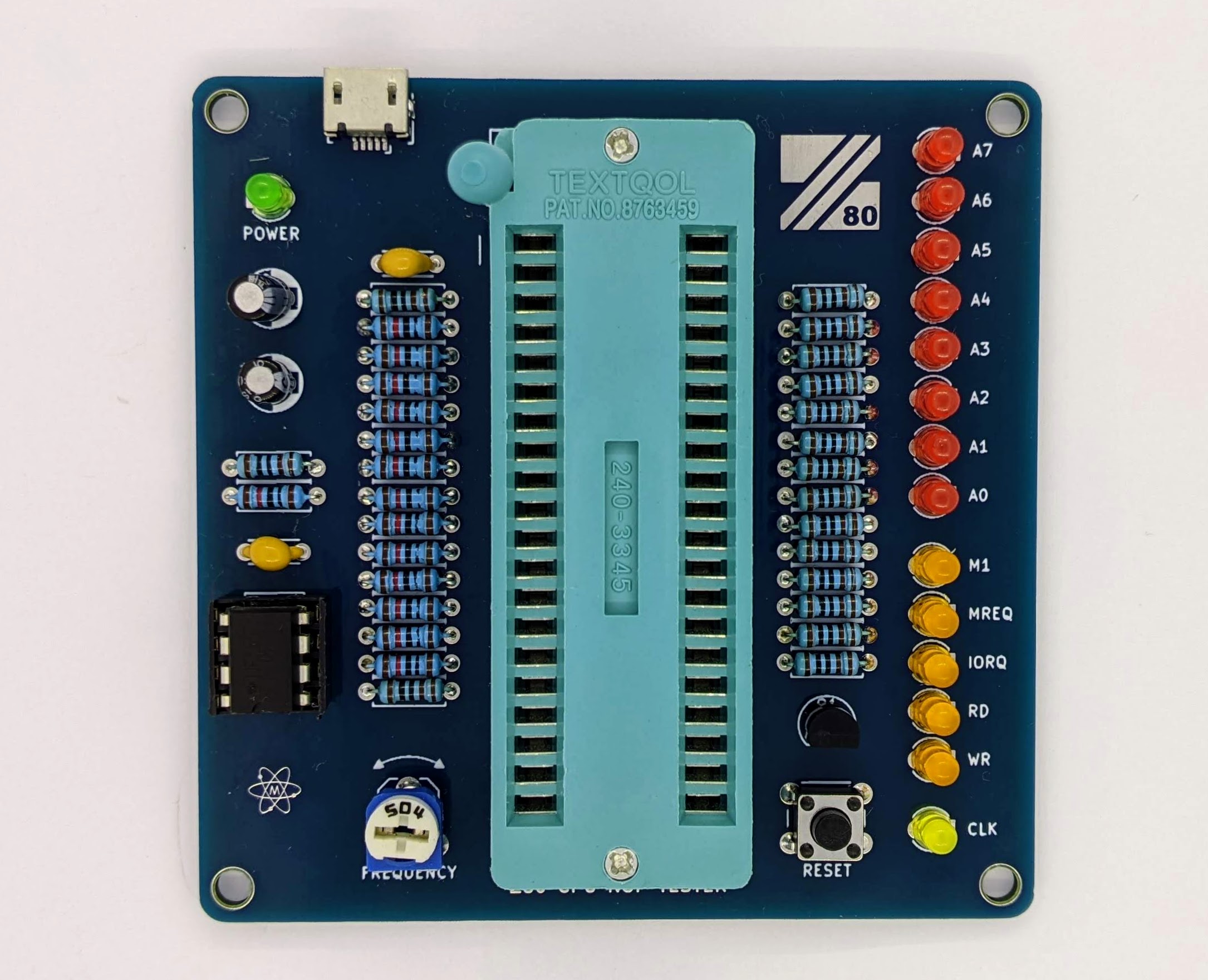
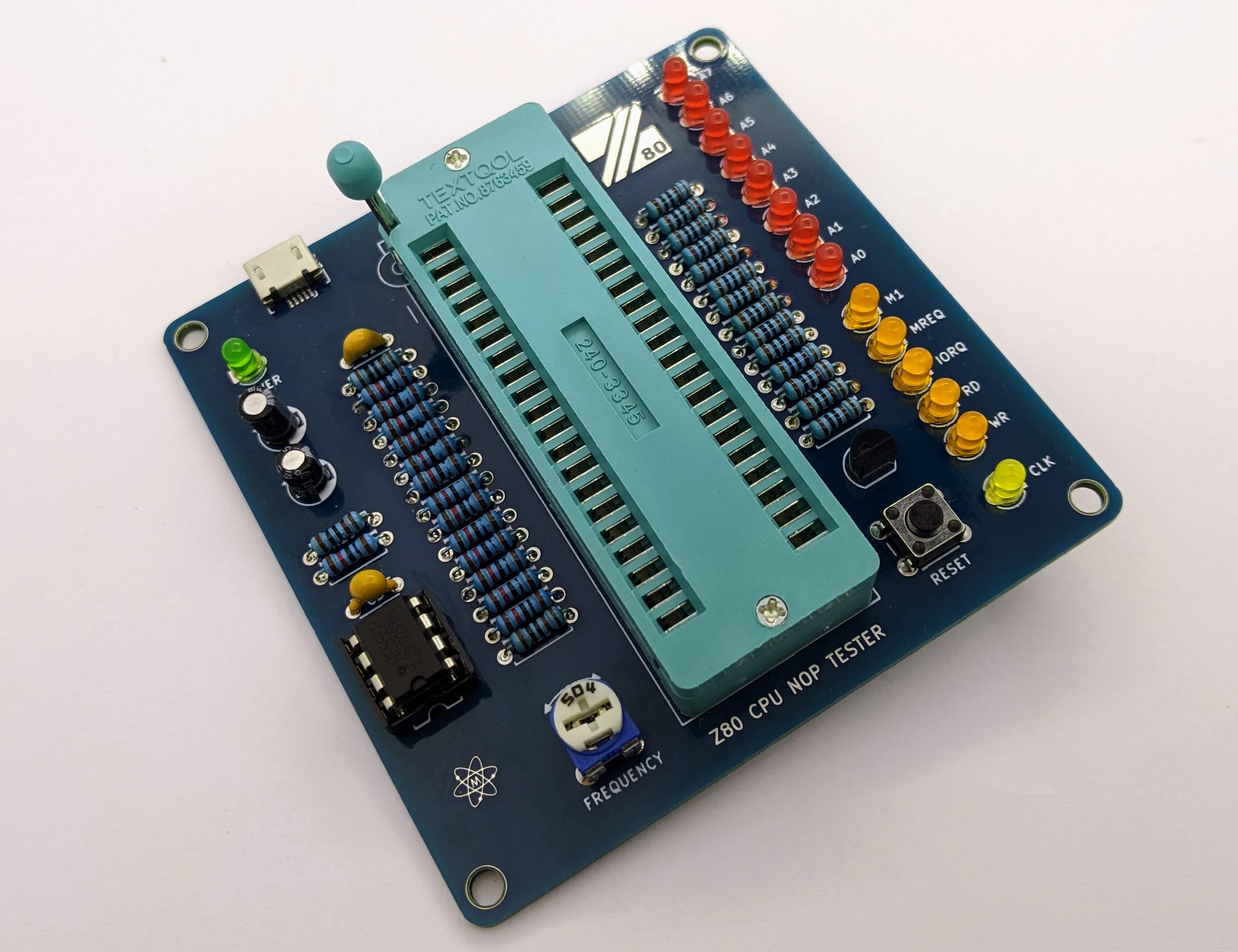
These boards look absolutely gorgeous in standard blue solder mask because hey! Zilog was all about blue! All components in BOM are standard offshelf parts with no special lead time. I bought mine on Ali.
┌( ͝° ͜ʖ͡°)=ε/̵͇̿̿/’̿’̿ ̿
Except where otherwise noted, content on this site is licensed under a Creative Commons Attribution 4.0 International license. CC-BY-4.0
I have created content on this website free to use for personal, educational and commercial purposes. If you like or use my work, please mention me or perhaps consider a donation.
| or |
... but if you feel like getting something for nothing isn't your cup of tea (completely understandable) (ಥ﹏ಥ) and a prefer to support me and get something back in return, then you can purchase directly on my eBay or Tindie shop. However if you are still up for an adventure */in very positive way/* (and are happy to have PCB's made yourself in your favourite PCB house - PCBWay is highly recommended), then carry on, download gerber files and have fun! ( ͡° ͜ʖ ͡°)


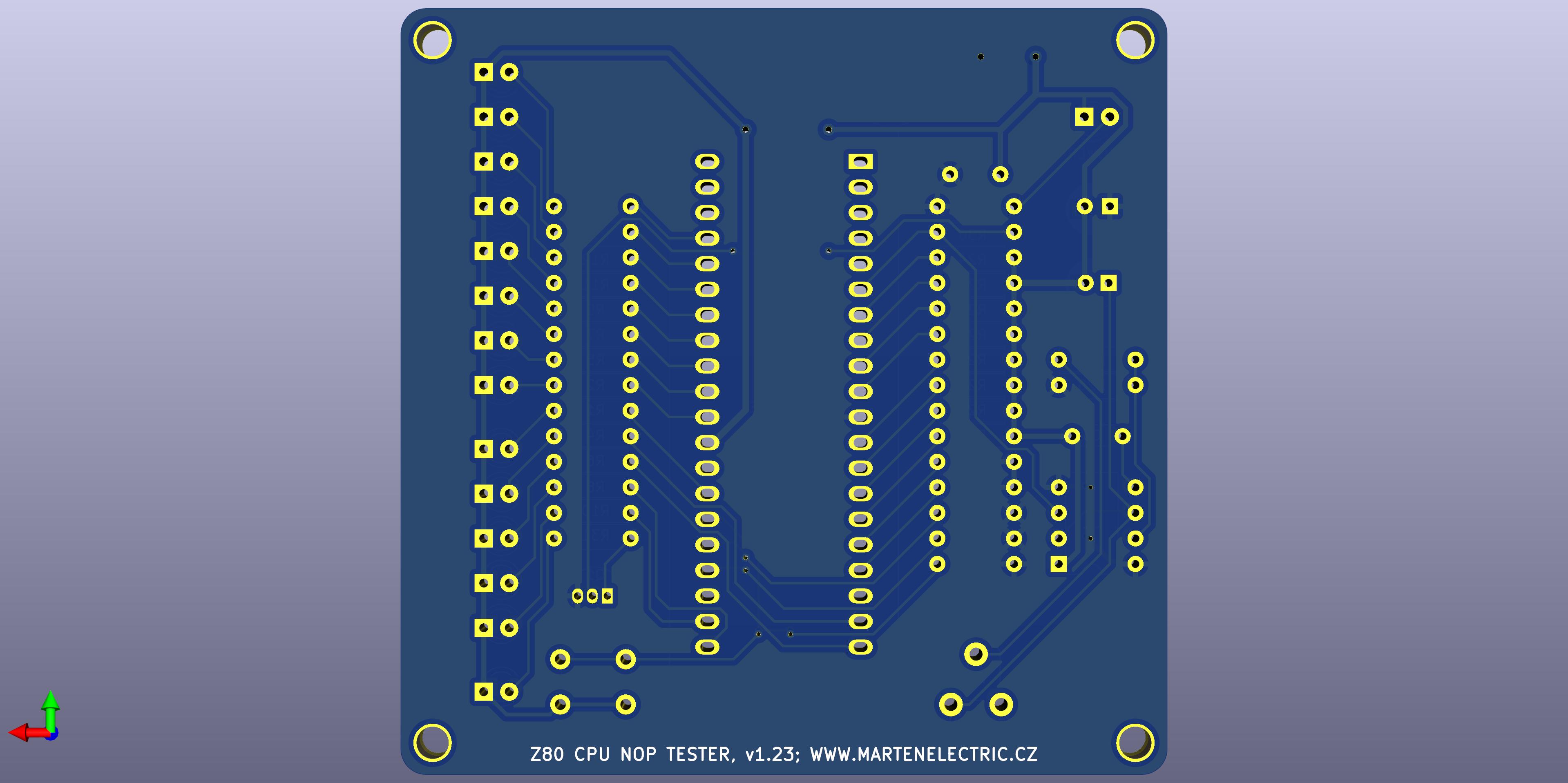
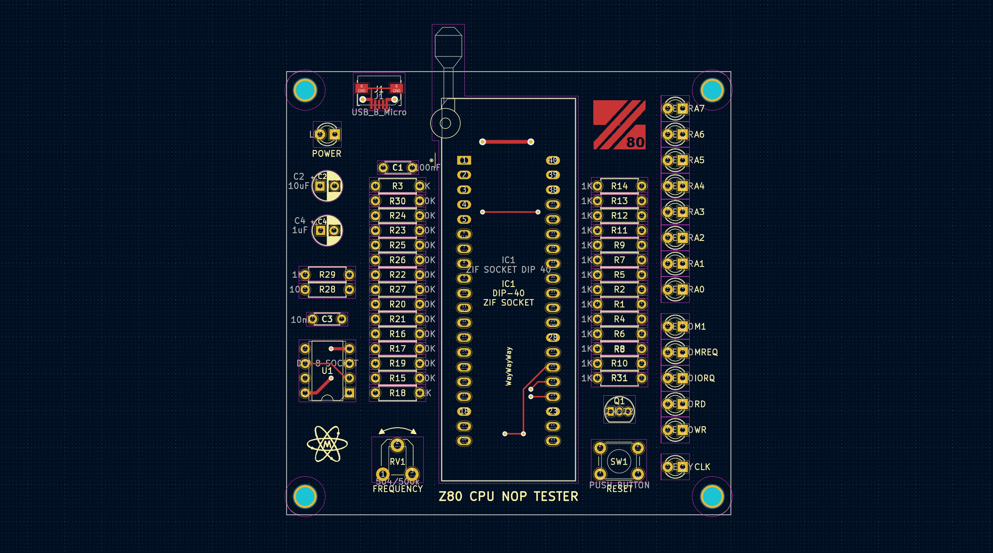
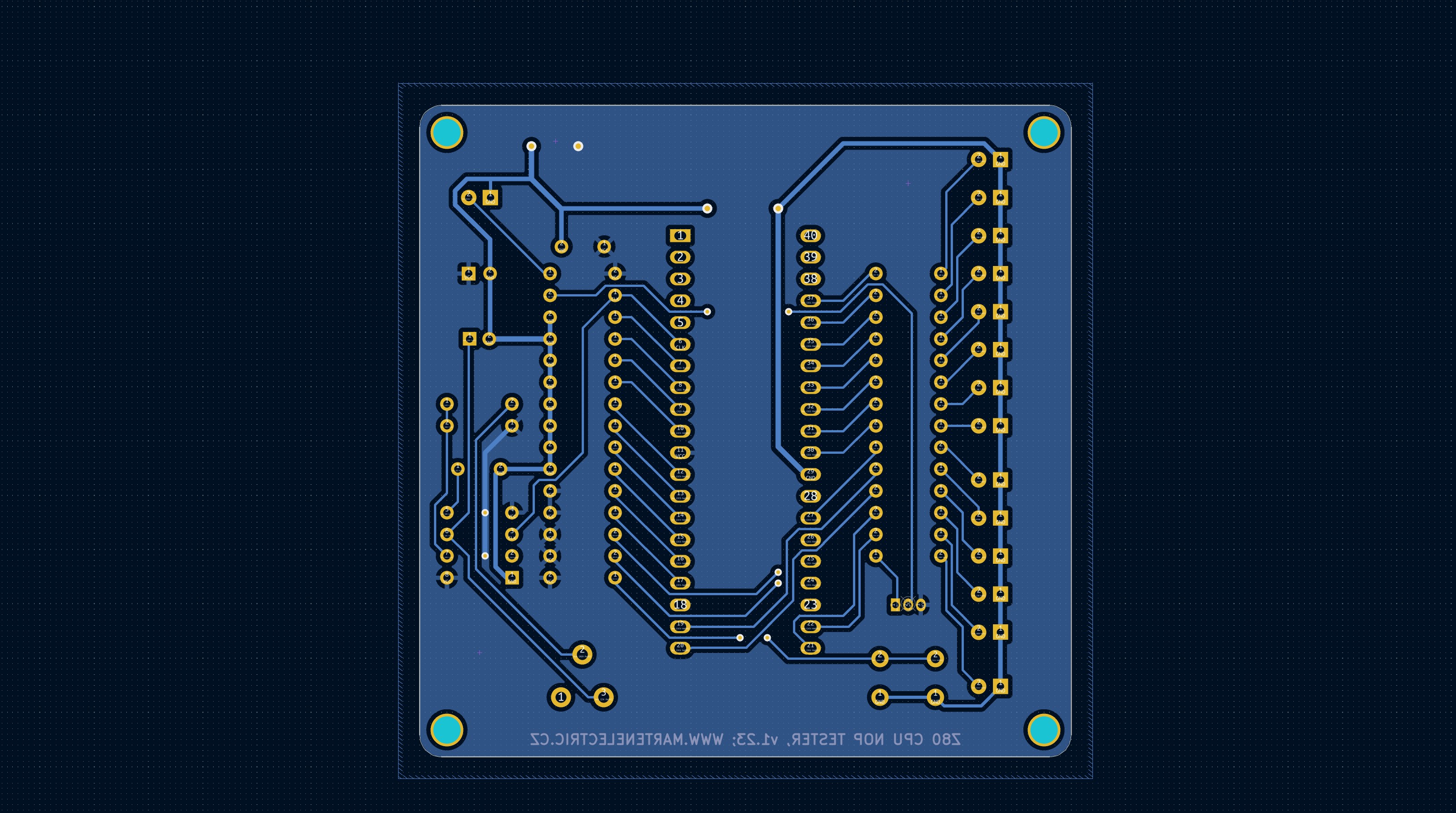
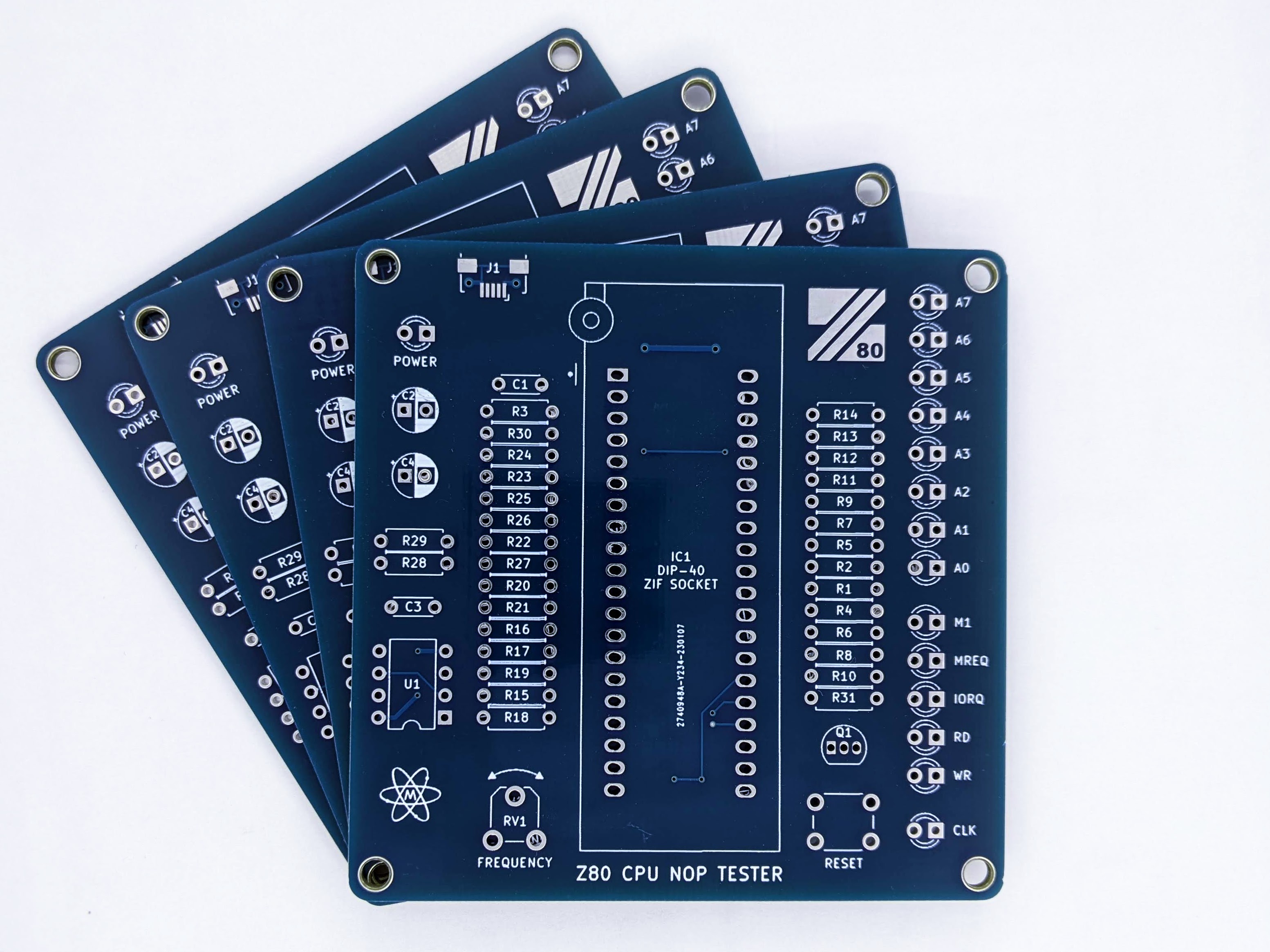
EDA preview
click on pictures to enlarge
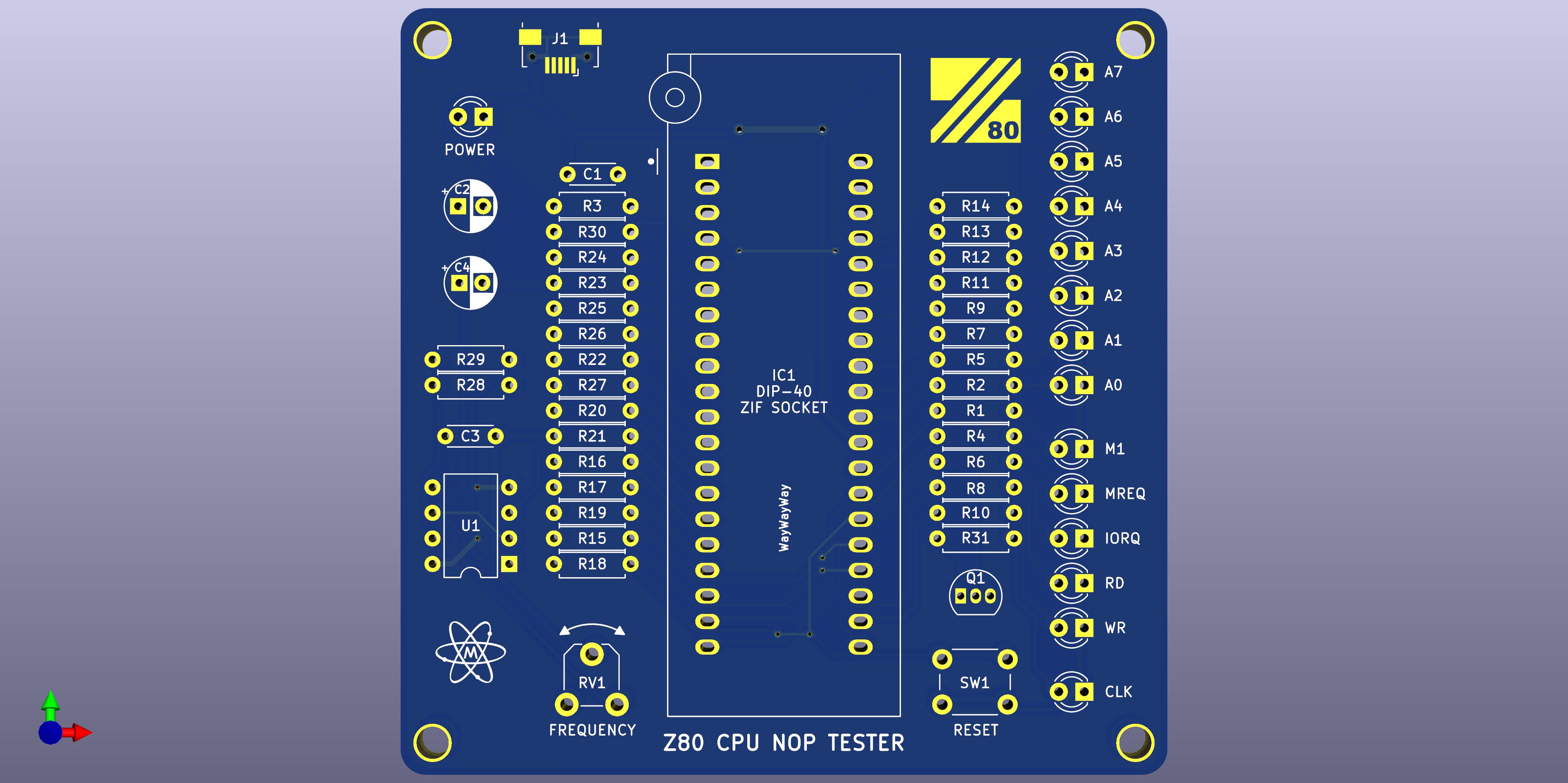
3d render v1.23
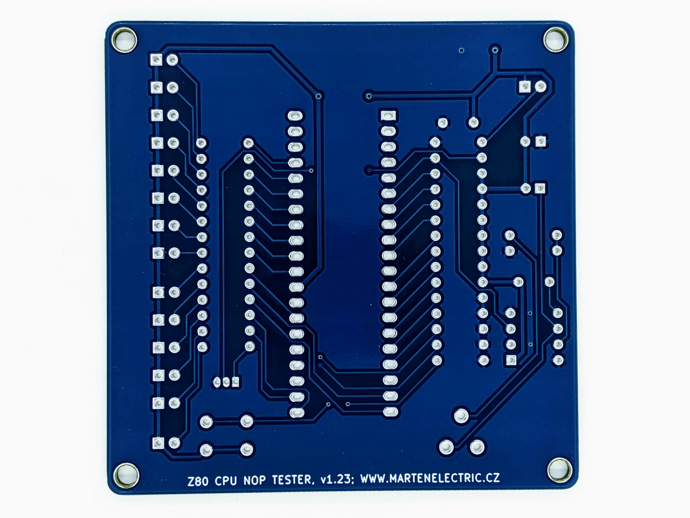
PCB design layout
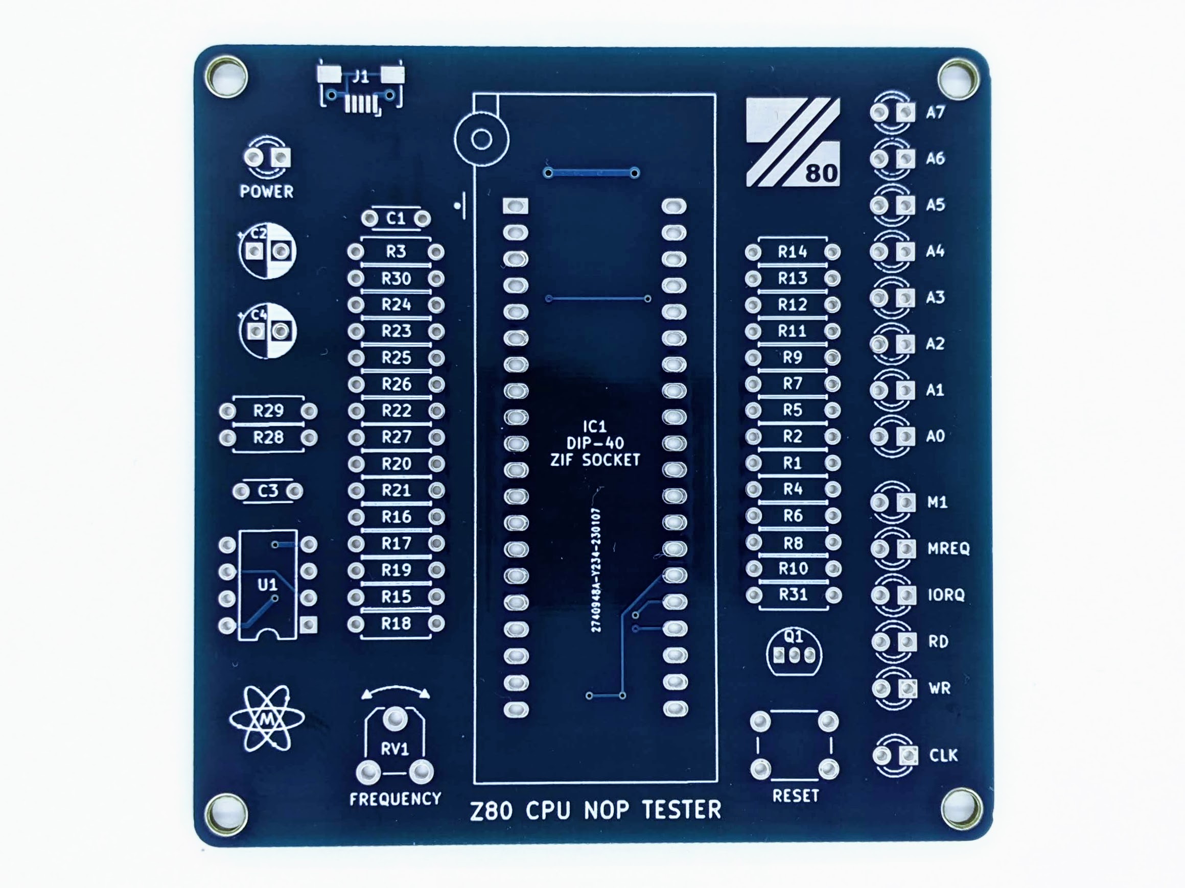
Specifications
Board Type: Tester
Board Material: FR4-Standard Tg 130-140C Epoxy Glass Composite
Layers: Double sided
PCB Colour: Blue colour solder mask, white silk screen lettering
Surface Finish: Lead free HASL-RoHS
External size (assembled): 76.2 x 76.2 x 15.0 mm
Board Thickness: standard 1.6mm
Copper Thickness: 35um
PCB weight: 10g
Asembled weight: 47g
Bill of materials
| Interactive HTML BOM |
|---|
| Convenient BOM listing with ability to visually correlate and easily search for components and their placements on the pcb. |
| Reference | Value | Footprint | Qty | Notes |
|---|---|---|---|---|
| Printed Circuit Board | PCB 76.2 x 76.2 mm, M3 mounting holes | 1 | v1.2 | |
| LED PWR | Green | LED_THT:LED_D3.0mm | 1 | |
| LED A0-A7 | Red | LED_THT:LED_D3.0mm | 8 | |
| LED M1-WR | Orange | LED_THT:LED_D3.0mm | 5 | |
| LED CLK | Yellow | LED_THT:LED_D3.0mm | 1 | |
| C1 | 100nF | Capacitor_THT:C_Disc_D4.3mm_W1.9mm_P5.00mm | 1 | |
| C2 | 10uF | Capacitor_THT:CP_Radial_D5.0mm_P2.50mm | 1 | |
| C3 | 10nF | Capacitor_THT:C_Disc_D4.3mm_W1.9mm_P5.00mm | 1 | |
| C4 | 1uF | Capacitor_THT:CP_Radial_D5.0mm_P2.50mm | 1 | |
| R1-R14,R18,R29,R31 | 1K | Resistor_THT:R_Axial_DIN0207_L6.3mm_D2.5mm_P7.62mm_Horizontal | 17 | |
| R15-R17,R19-R28,R30 | 10K | Resistor_THT:R_Axial_DIN0207_L6.3mm_D2.5mm_P7.62mm_Horizontal | 14 | |
| Q1 | 2N222 | Package_TO_SOT_THT:TO-92_Inline | 1 | NPN Transistor, Alternative 2N3904 |
| SW1 | Reset | Button_Switch_THT:SW_PUSH_6mm_H5mm | 1 | Momentary Push Button Switch |
| RV1 | 500K / 504 | Potentiometer_THT:Potentiometer_ACP_CA9-H5_Horizontal | 1 | Frequency adjust |
| U1 | NE555 | Package_DIP:DIP-8_W7.62mm | 1 | Precision timer monostable NE555 / LM555 Datasheet |
| U1 | DIP 8 | Package_DIP:DIP-8_W7.62mm | 1 | Socket |
| IC1 | ZIF | Socket:DIP_Socket-40_W11.9_W12.7_W15.24_W17.78_W18.5_3M_240-1280-00-0602J | 1 | DIP40 ZIF Socket, any DIP40 socket can be used |
| J1 | USB_B_Micro | Connector_USB:USB_Micro-B_Amphenol_10118194_Horizontal | 1 | |
| Components in total | 57 |
Assembly instructions and notes
■ Gerber files contain " WayWayWay" to the silk layer. You can specify a location of the order number, select the "Specify a location" option when you place an order. Only if you order via PCBWay.
■ Use a temperature-controlled soldering station and quality solder, use plenty of flux. Take care not to leave solder bridges as any short circuit will most likely lead to failures
■ Use a temperature-controlled heat gun station and quality solder paste, use plenty of flux. Take care not to leave solder bridges as any short circuit will most likely lead to failures
■ Use quality ZIF Socket for CPU, alternative machined socket with golden plated pin headers is recommended, they are rather cheap and will protect your precious DIP socket. 555 timer can be soldered directly, however little DIP8 socket is recommended.
■ Use little screwdriver to adjust frequency of 555 Timer
■ Tip for testing GDR ( East-Germany ) CPU´s ( U880D, UA880D, UB880D ). When testing GDR CPU´s, it has happened that some of them are apparently defective. The real reason, however, is the grid dimension, international 2,54 mm and GDR 2,5 mm, there are contact problems with the Textool-Socket 2,54 mm pitch. The remedy is to insert a 40-pin socket 2,54 mm pitch between. Now all my East-Germany CPU´s work !
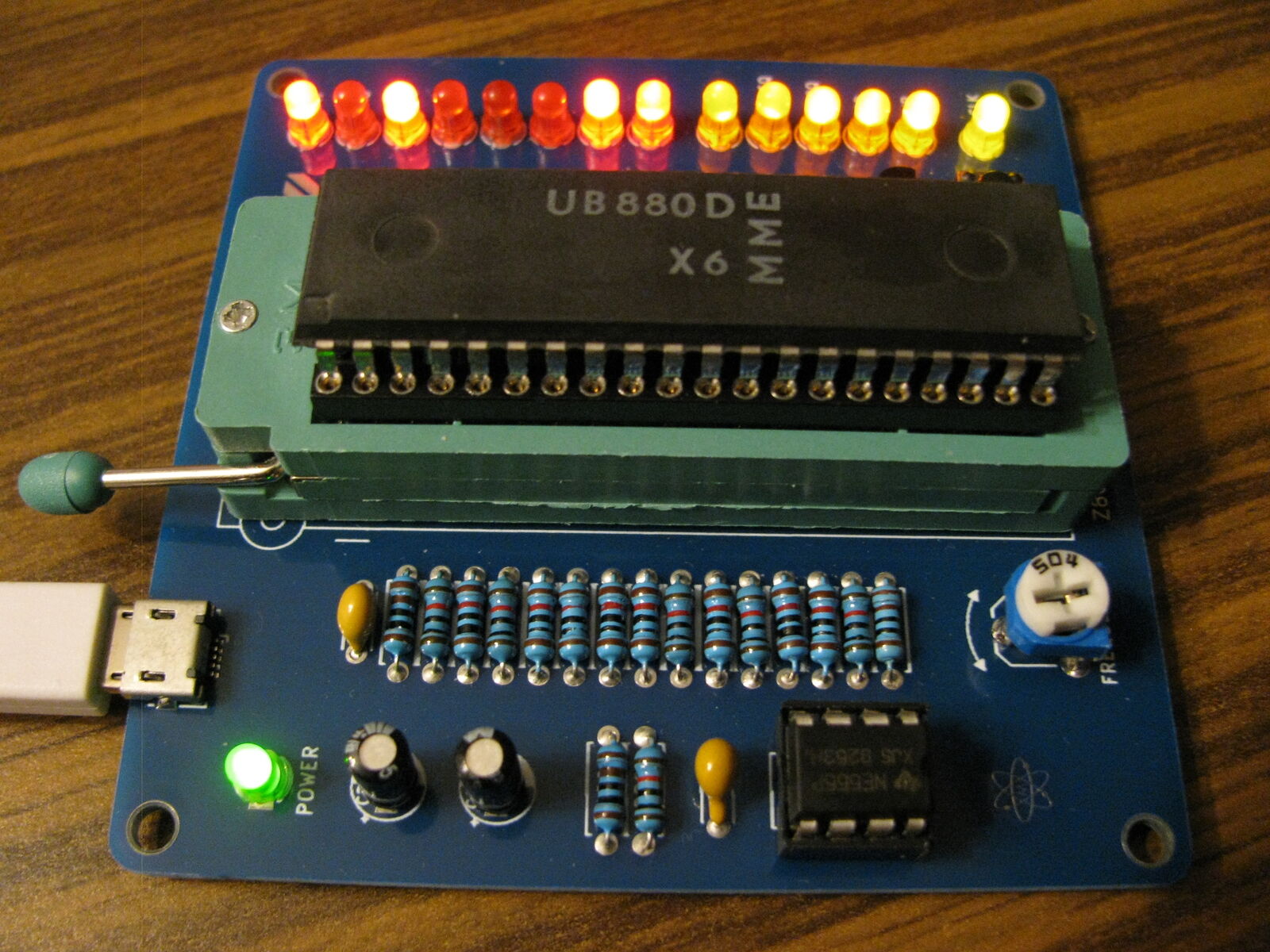
Photograph by Frank Wegner (c) 2023
■ Assembly:
1 - First start with USB B connector: Hold socket in place and dab a bit of solder on the little connector, it's fiddly due to the nature and size of SMD components so you might want to use a solder wick if you overdo it. Test for solder bridges just in case. Alternatively use solder paste and hot air.
2 - Start from the physically lowest component: Resistors, caps, LEDs, transistor, button etc. Solder ZIF socket as a last component.
3 - Clean the flux residue and crap with IPA
4 - Test for voltages prior to first use, just in case... because the last thing you want is to fry your CPU
5 - Insert CPU, plug in USB power plug and Enjoy!
■ How to test the CPU:
1 - Slot the Zilog Z80 CPU into the ZIF socket. CPU should fall into the ZIF socket without force.
2 - Please Make sure the Z80 is inserted correctly. Pin 1 CPU is top left by the lever.
3 - Power up the CPU tester by inserting a Mini USB Type B cable from the PC or use standard +5VDC USB phone charger.
4 - Press Reset button. CPU starts from zero count state.
5 - Fiddle with the potentiometer to achieve the clock speed you require for your experiments.
6 - Enjoy!
Schematic
| File type | File name | File size | Last modified |
|---|---|---|---|
| Z8400 CPU Product specification, document PS017801-0602, Fig2,2a,2b | 1124 kB | 20/07/2021 | |
| Z80 CPU PLCC44 to DIP40 adapter Schematic v1.0 | 84 kB | 19/09/2021 |
Design Files
| File type | File name | File size | Last modified |
|---|---|---|---|
| Instruction manual v1.0 | 2104 kB | 03/04/2025 | |
| PCB layers v1.21 | 199 kB | 19/08/2022 | |
| BOM and Component placement v1.22 Interactive HTML BOM | 281 kB | 04/10/2022 | |
| BOM and Component placement v1.2 | 166 kB | 04/06/2022 | |
| Component placement v1.2 | 25 kB | 03/06/2022 | |
| Gerbers 76.2 x 76.2 mm, 2 Layer FR4, v1.21 | 127 kB | 19/08/2022 | |
| Gerbers 76.2 x 76.2 mm, 2 Layer FR4, v1.23 | 250 kB | 06/01/2023 | |
| Solder paste stencil | Not available for this project | - | - |
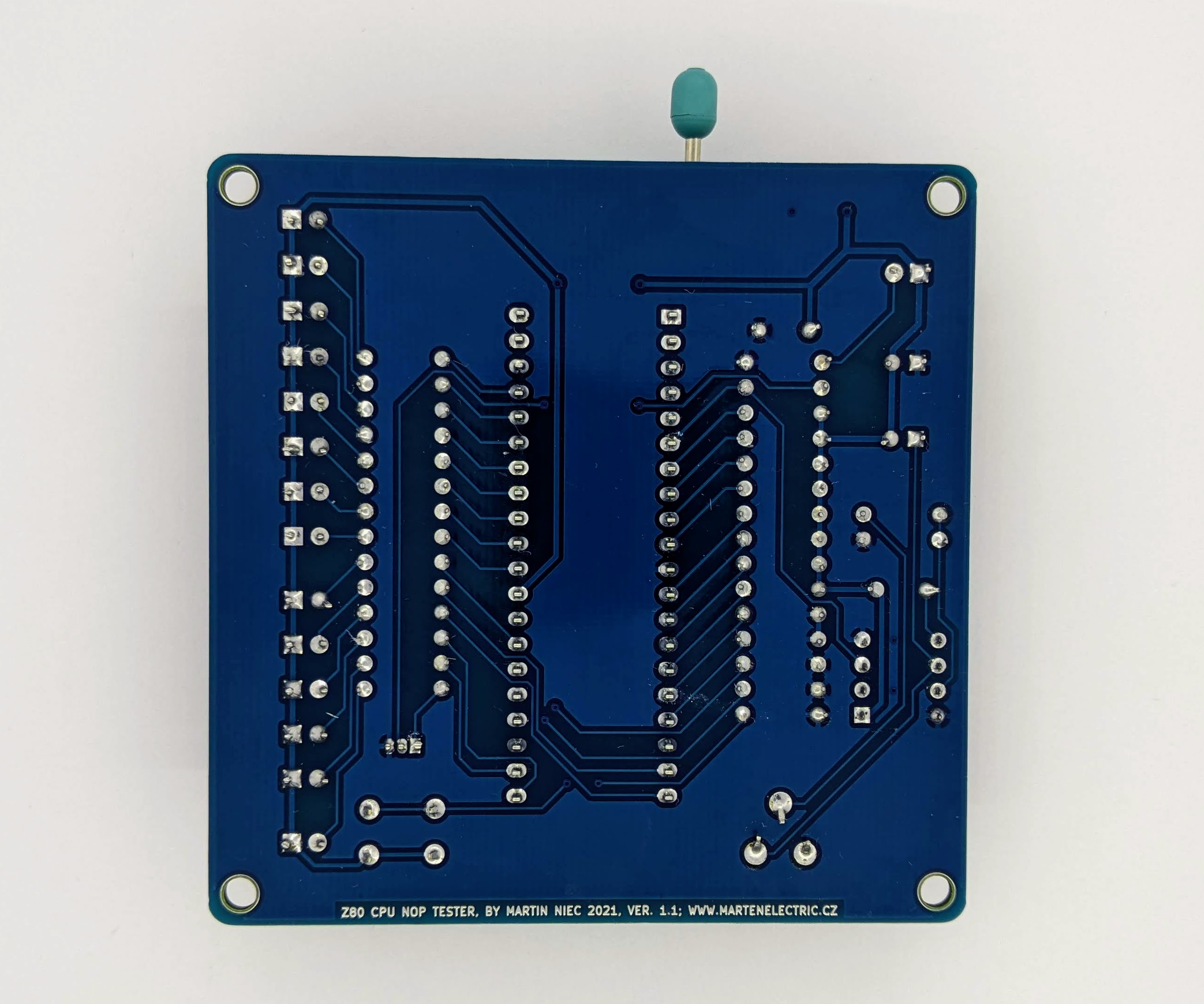
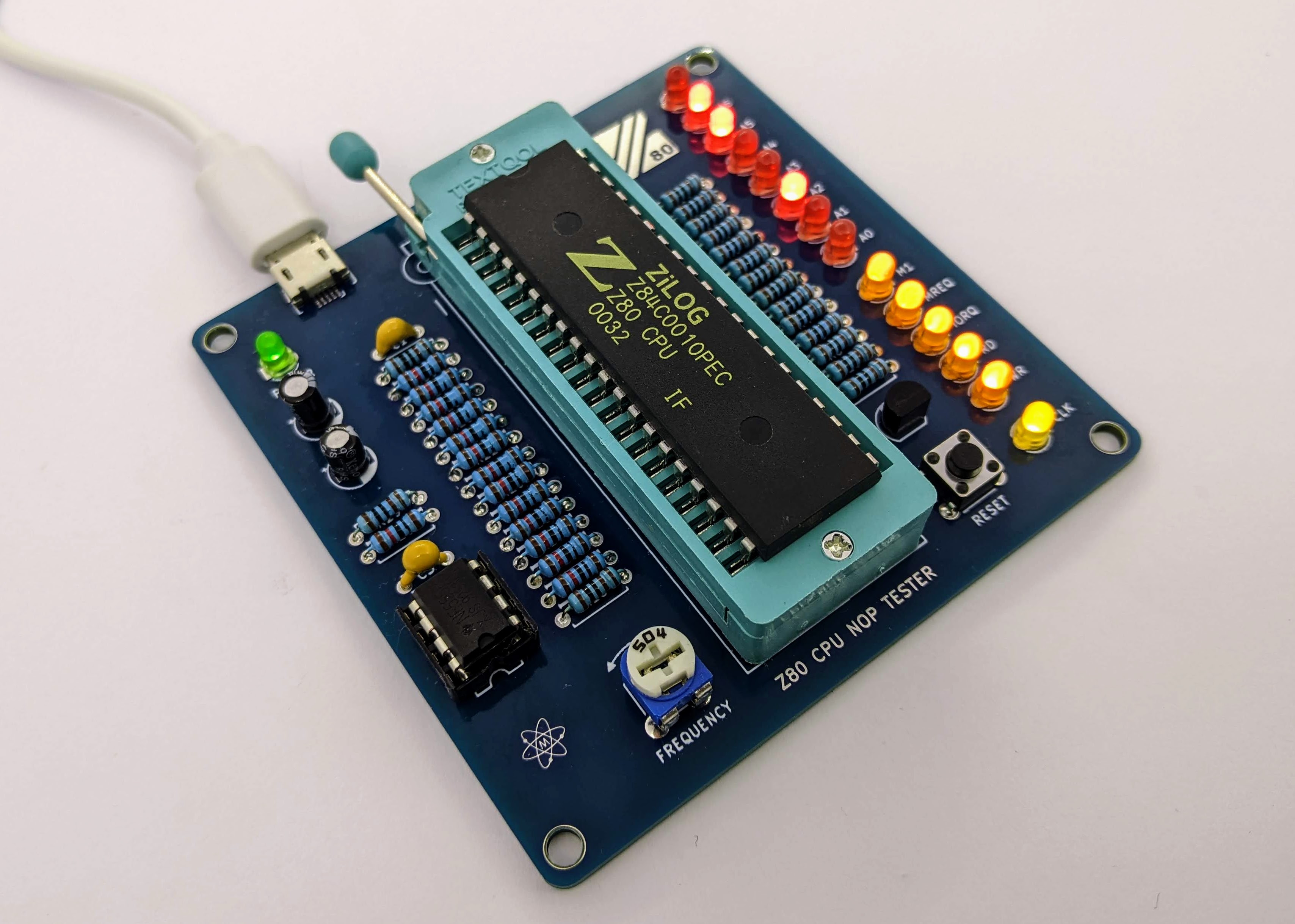
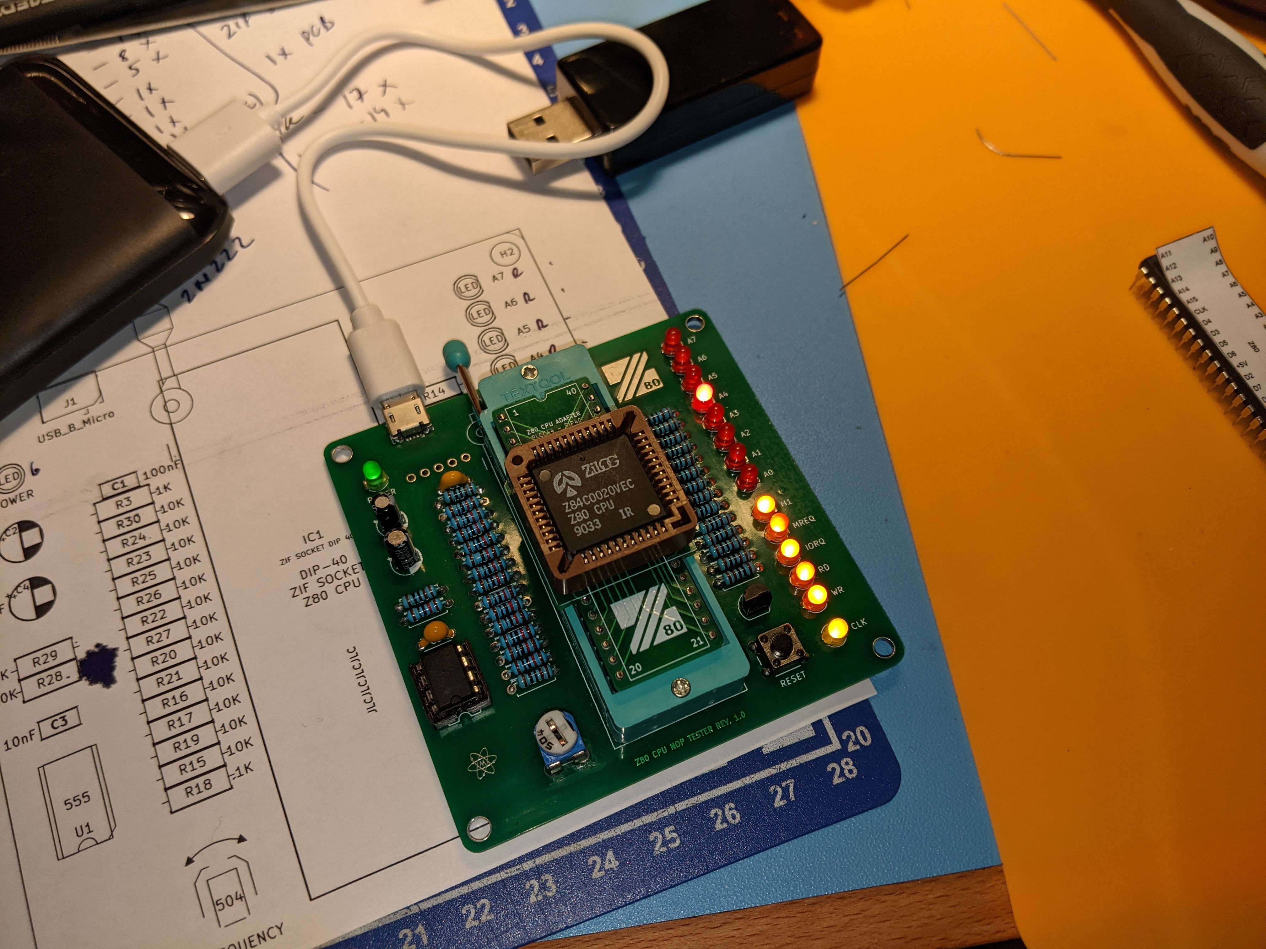
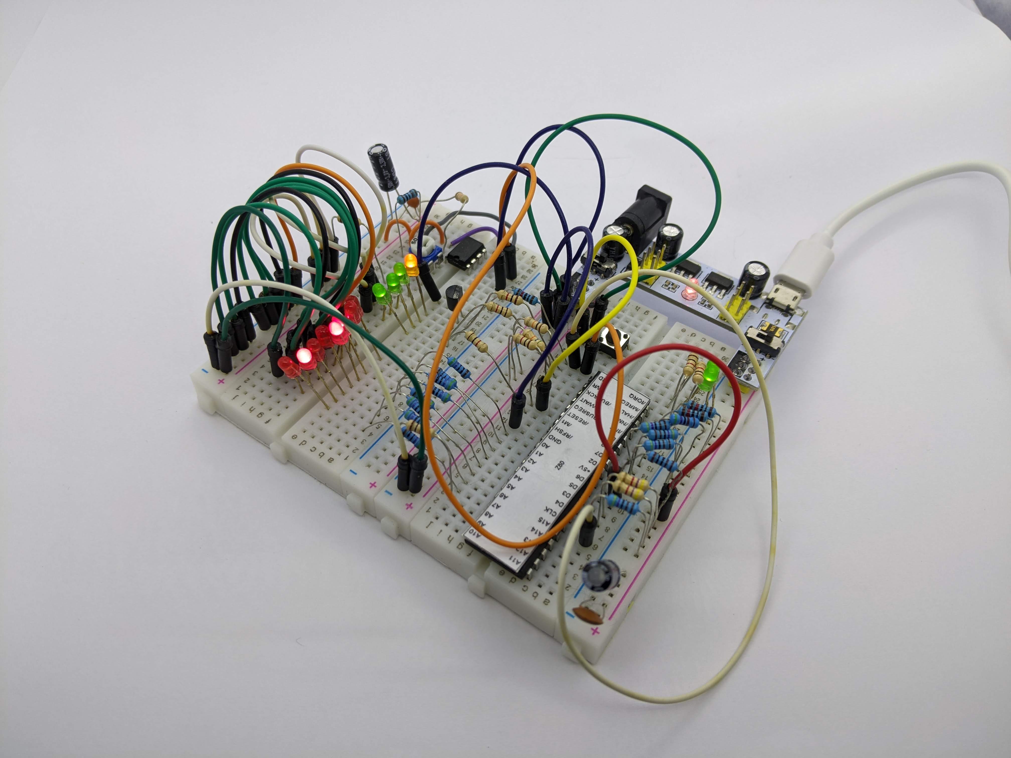
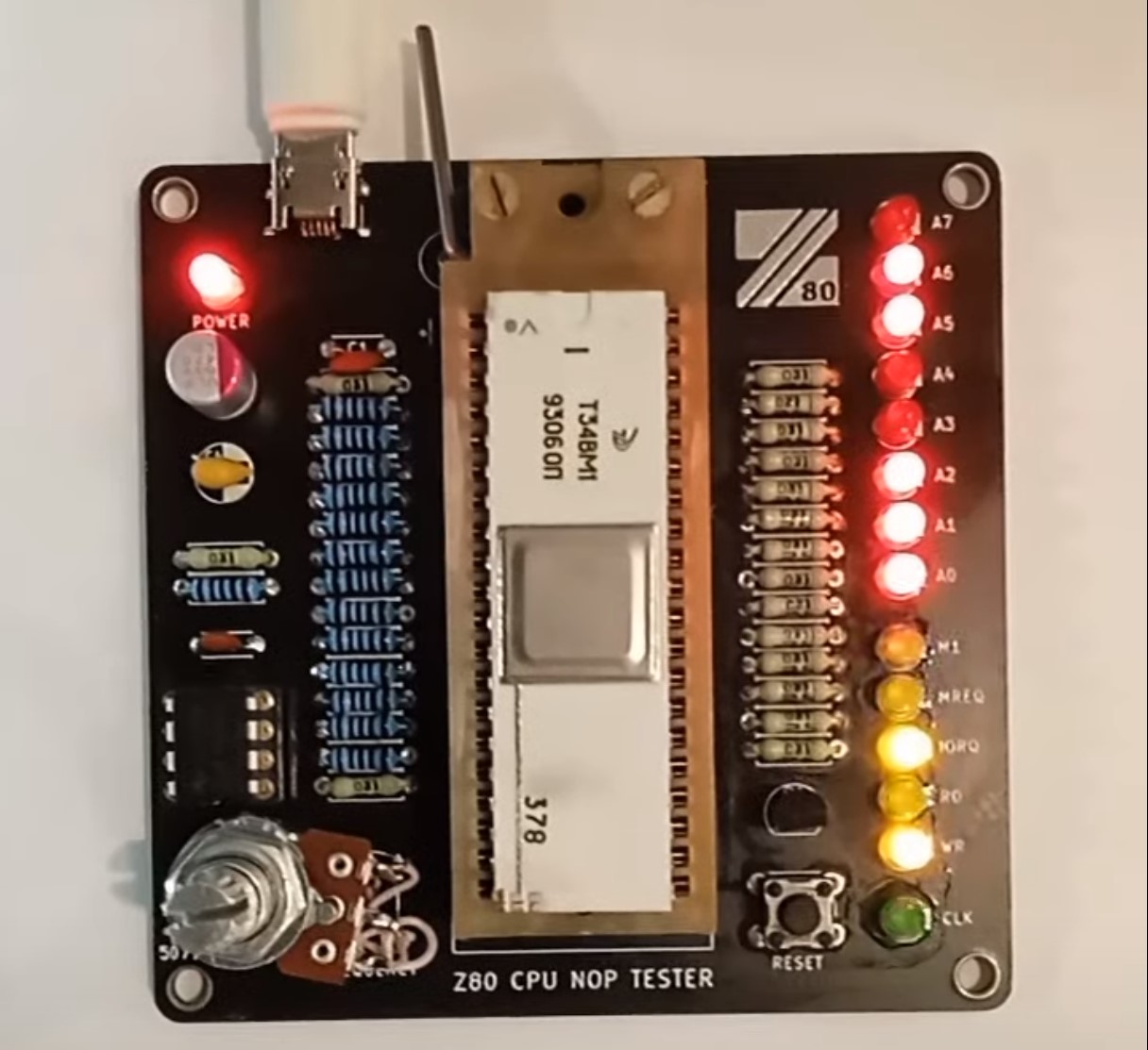
Photographs
click on pictures to enlarge
gerber files and photographs may vary, v1.23 pictured
gerber files and photographs may vary, v1.1 pictured
gerber files and photographs may vary, v1.0 (rev.0) pictured
Z80 tester with Т34ВМ1 (T34VM1) Soviet clone of Z80 CPU. Photograph by Г. Саратов
Versions and revisions
This section lists the project version and revision history.
v1.23
■ Silk screen update
■ Power LED Footprint update - Footprint flipped horizontally to match other LEDs anode orientation
v1.21
■ Silk screen update
■ Large pad holes for ZIF socket
■ Q1 Footprint update
v1.2
■ Various Copper and cosmetic updates
■ Reference designators added
v1.1
■ USB B connector position corrected
■ Various silkscreen updates
■ Various cosmetic updates
v1.0
■ prototype